

Electromagnetics Plasma Simulation
Plasma Etching Simulation
Simulation of Plasma Based Devices: Microwave Plasma & RF Plasma with Coupling Particle in Cell (PIC), MHD, CFD and FEA Solvers
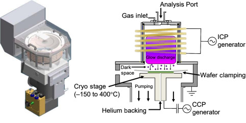
Plasma etching is an essential tool in today's world, enabling many of the technologies we take for granted. The chemical nature of a process gas dictates how its plasma reacts with the surface of a material and therefore the effectiveness of plasma etching. For instance, tetrachloromethane (CCl4) etches silicon and aluminium effectively but the plasma etching of silicon dioxide and silicon nitride requires the use of trifluoromethane (CHF3). Native oxide layers, on the other hand, can be removed from a titanium surface by argon plasma etching. Other examples of plasma etching as a means of surface preparation for biomedical coatings.
Inductively Coupled Plasma Reactive-Ion Etching (ICP-RIE):
Inductively coupled plasma reactive ion etching (ICP-RIE) is used in the fabrication of GaAs slab-coupled optical waveguide (SCOW) laser and amplifier devices in order to prepare etched-ridge-waveguide surface features. The processing of GaAs wafer pieces (less than full wafers) requires mounting these samples on a ceramic or silicon carrier wafer by means of a thermally conductive mounting paste to improve thermal contact between the GaAs and carrier wafer. However, use of a mounting paste requires additional postetch handling of samples, including mechanical clean-up and multiple solvent cleaning steps. Insufficient paste removal can lead to unwanted surface contamination and film adhesion issues during subsequent sample processing.
Reactive Ion Etching (RIE):
Reactive ion etching (RIE) is a plasma process where radiofrequency (RF) discharge-excited species (radicals, ions) etch substrate or thin films in a low-pressure chamber. RIE is a synergistic process between chemically active species and energetic ion bombardment. RIE is faster than either pure physical ion bombardment or spontaneous chemical etching. Understanding the consequences of local surface charging on the evolving etching profile is a critical challenge in high density plasma etching. Deflection of the positively charged ions in locally varying electric fields can cause profile defects such as notching, bowing, and microtrenching.
A realistic process simulation therefore needs to consider these interactions, which makes the numerical simulation more challenging. Suitable numerical methods or adequate approximations are crucial for the simulation of feedback and interactions.
Plasma Simulation
OLTRION uses advanced electromagnetic FEA, CFD and particle-in-cell (PIC) codes, designed for executing multi-scale, plasma physics simulations. Based on the problem and its detail, we use special commercial …
Capabilities that sit beside this one
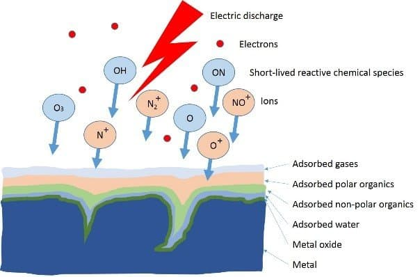 Plasma Cleaning
The operational cost of using plasma cleaning systems are low, while providing the highest quality in cleaning surfaces. Another benefit of using …
Open capability
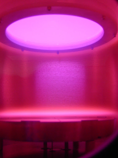 Plasma-enhanced chemical vapor deposition (PECVD)
Plasma-enhanced chemical vapor deposition coating: Plasma-enhanced chemical vapor deposition (PECVD) is a thin-film deposition technique that allows for tunable control over the …
Open capability
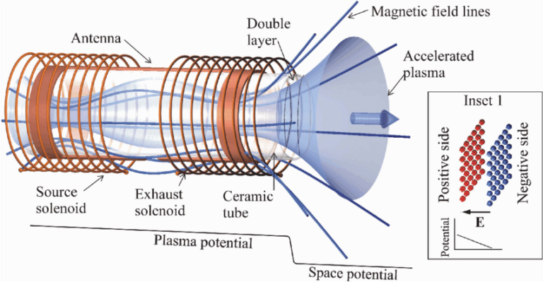 Simulation Based Design of Plasma Thrusters
Electric propulsion technology, called Hall effect or stationary plasma thrusters, offers a significant weight reduction compared with traditional chemical propulsion systems. In …
Open capability
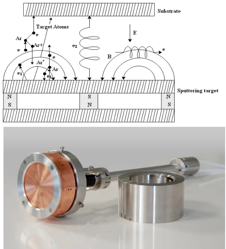 Numerical Simulation of Magnetron sputtering
Magnetron sputtering deposition is a fast technique for applying a thin layer of inorganic materials on a substrate. Magnetron sputtering is the …
Open capability
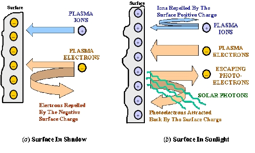 Spacecraft and Satellite charging effects Numerical Simulation
Spacecraft charging includes both surface charging and internal dielectric charging. The absolute charging of spacecraft surfaces is not generally detrimental; rather it …
Open capability
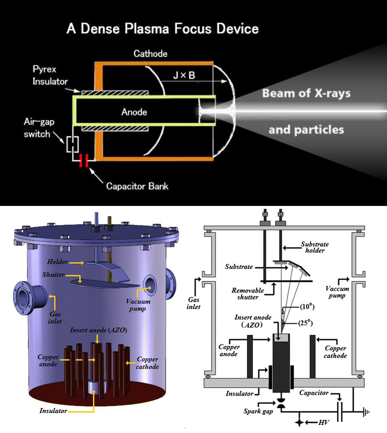 Numerical Simulation of Dense Plasma Focus Devices
A dense plasma focus (DPF) is a plasma machine that produces, by electromagnetic acceleration and compression, short-lived plasma that is so hot …
Open capability
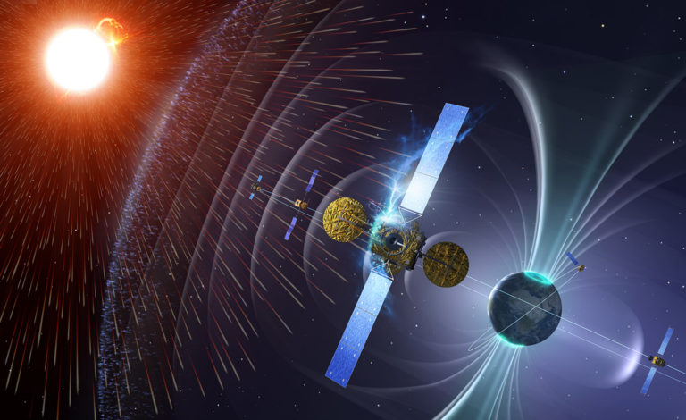 Spacecraft Shielding
Traditional methods for protecting spacecraft and occupants from harmful radiation in the form of energetic particles from solar and galatic sources involve …
Open capability
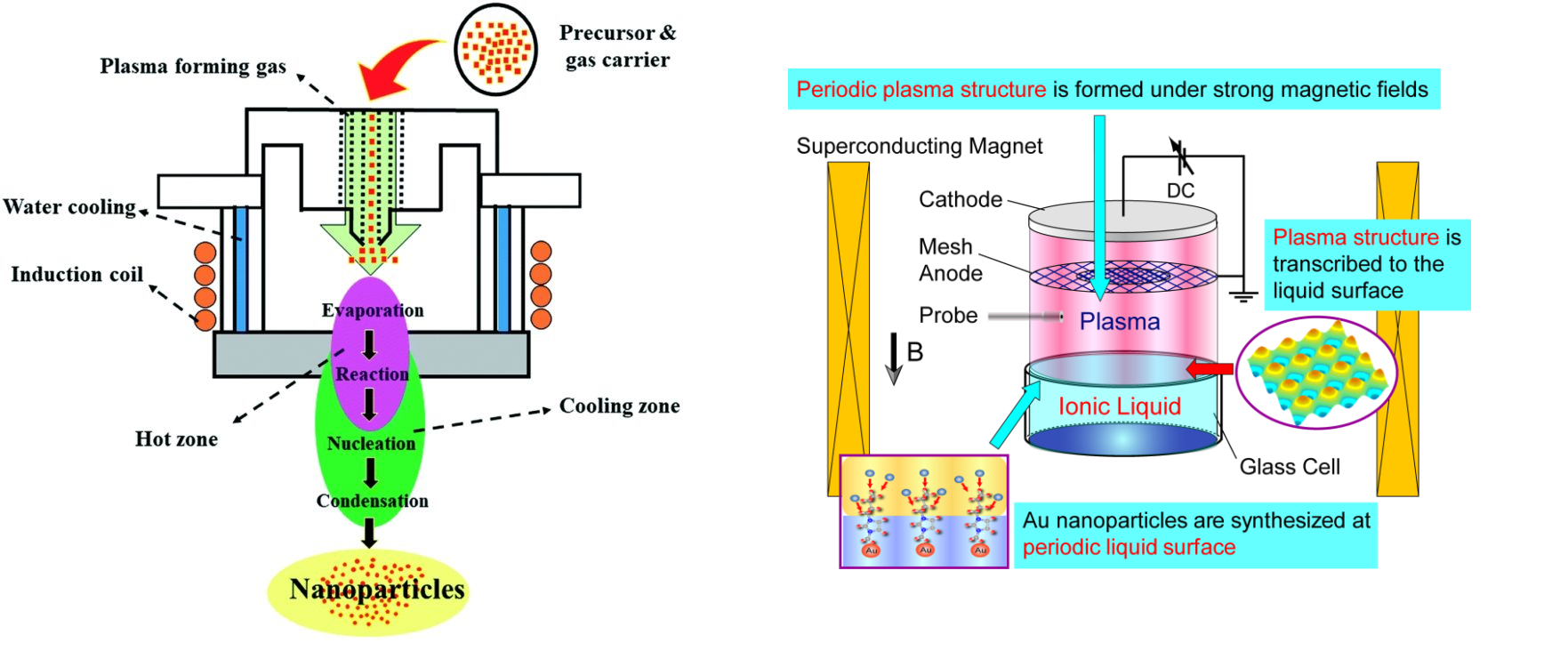 Nanoparticle Synthesis Simulation Based Design
Plasma-based chemical processes are characterized by solvent-less (dry), high-purity, and low-temperature conditions that enable damage-free device fabrication. plasma tools are now essential …
Open capability
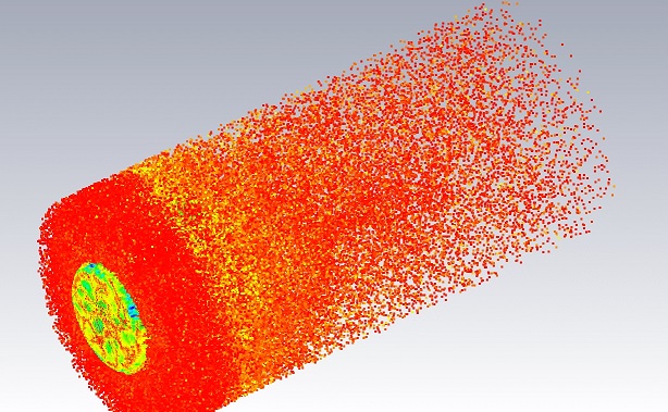 Simulation of Plasma Based Devices
We provide consulting services for the modeling and simulation of plasma and other flow systems. we combine expertise in physics, Numerical computing, …
Open capability
Other Simulation Area
Working on plasma etching simulation?
Tell us the geometry, the physics and the decision it has to support.
Talk to an engineer